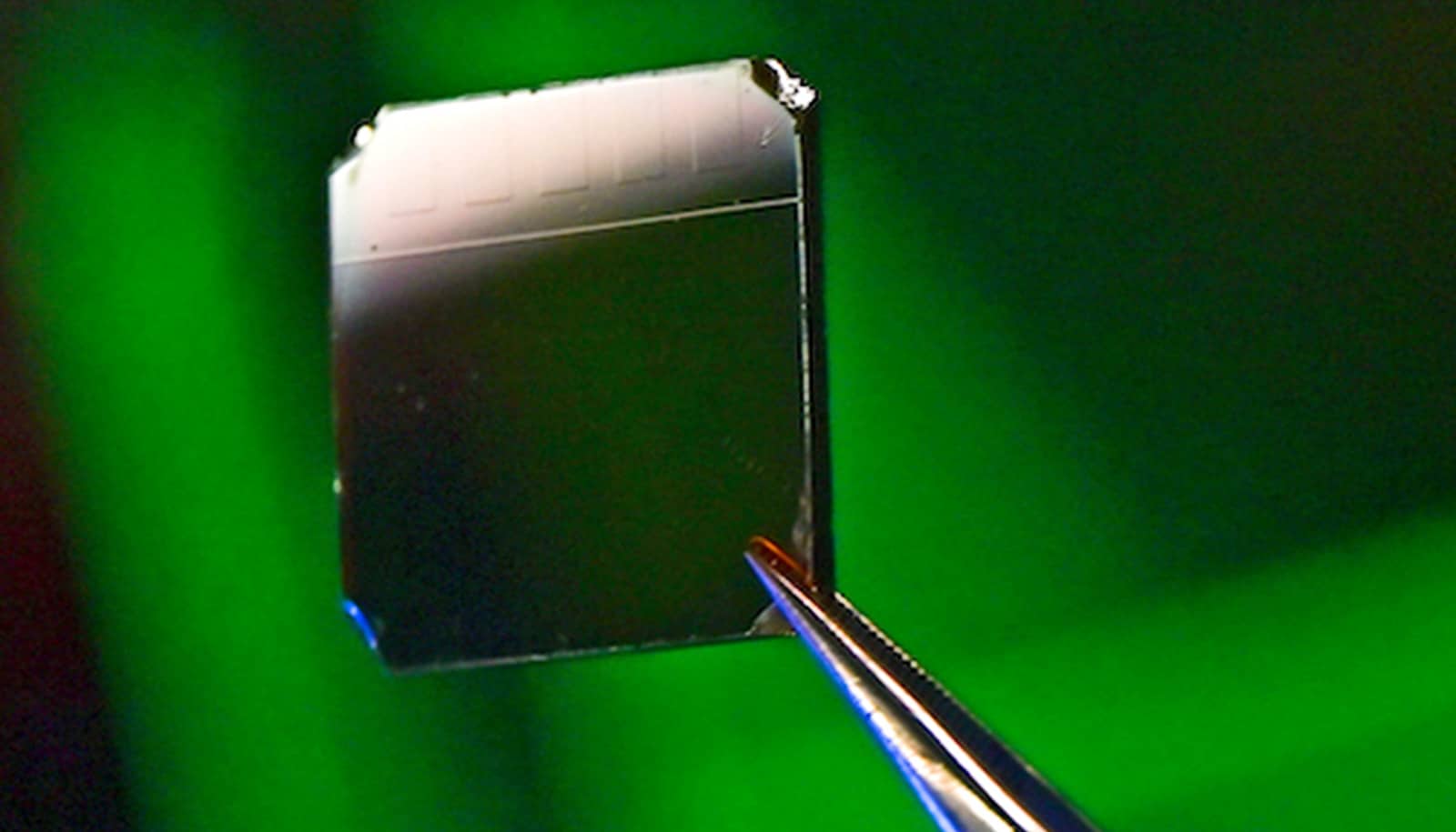
Researchers have achieved a new benchmark in the design of atomically thin solar cells made of semiconducting perovskites, boosting their efficiency while retaining their ability to stand up to the environment.
The lab of Aditya Mohite of Rice University’s George R. Brown School of Engineering discovered that sunlight itself contracts the space between atomic layers in 2D perovskites enough to improve the material’s photovoltaic efficiency by up to 18%, an astounding leap in a field where progress is often measured in fractions of a percent.
“In 10 years, the efficiencies of perovskites have skyrocketed from about 3% to over 25%,” Mohite says. “Other semiconductors have taken about 60 years to get there. That’s why we’re so excited.”
Perovskites are compounds that have cubelike crystal lattices and are highly efficient light harvesters. Their potential has been known for years, but they present a conundrum: They’re good at converting sunlight into energy, but sunlight and moisture degrade them.
“A solar cell technology is expected to work for 20 to 25 years,” says Mohite, an associate professor of chemical and biomolecular engineering and of materials science and nanoengineering. “We’ve been working for many years and continue to work with bulk perovskites that are very efficient but not as stable. In contrast, 2D perovskites have tremendous stability but are not efficient enough to put on a roof.
“The big issue has been to make them efficient without compromising the stability,” he says.
The researchers discovered that in certain 2D perovskites, sunlight effectively shrinks the space between the atoms, improving their ability to carry a current.
“We find that as you light the material, you kind of squeeze it like a sponge and bring the layers together to enhance the charge transport in that direction,” Mohite says. The researchers found placing a layer of organic cations between the iodide on top and lead on the bottom enhanced interactions between the layers.
“This work has significant implications for studying excited states and quasiparticles in which a positive charge lies on one layer and the negative charge lies on the other and they can talk to each other,” Mohite says. “These are called excitons, which may have unique properties.
“This effect has given us the opportunity to understand and tailor these fundamental light-matter interactions without creating complex heterostructures like stacked 2D transition metal dichalcogenides,” he says.
Colleagues in France confirmed the experiments with computer models. “This study offered a unique opportunity to combine state of the art ab initio simulation techniques, material investigations using large scale national synchrotron facilities, and in-situ characterizations of solar cells under operation,” says Jacky Even, a professor of physics at the Institute of Electronics and Digital Technologies (INSA) in Rennes, France. “The paper depicts for the first time how a percolation phenomenon suddenly releases the charge current flow in a perovskite material.”
Both results showed that after 10 minutes under a solar simulator at one-sun intensity, the 2D perovskites contracted by 0.4% along their length and about 1% top to bottom. They demonstrated the effect can be seen in 1 minute under five-sun intensity.
“It doesn’t sound like a lot, but this 1% contraction in the lattice spacing induces a large enhancement of electron flow,” says graduate student and co-lead author Wenbin Li. “Our research shows a threefold increase in the electron conduction of the material.”
At the same time, the nature of the lattice made the material less prone to degrading, even when heated to 80 degrees Celsius (176 degrees Fahrenheit). The researchers also found the lattice quickly relaxed back to its normal configuration once the light was turned off.
“One of the major attractions of 2D perovskites was they usually have organic atoms that act as barriers to humidity, are thermally stable, and solve ion migration problems,” says graduate student and co-lead author Siraj Sidhik. “3D perovskites are prone to heat and light instability, so researchers started putting 2D layers on top of bulk perovskites to see if they could get the best of both.
“We thought, let’s just move to 2D only and make it efficient,” he says.
To observe the material contraction in action, the team made use of two US Department of Energy (DOE) Office of Science user facilities: the National Synchrotron Light Source II at DOE’s Brookhaven National Laboratory and the Advanced Photon Source (APS) at DOE’s Argonne National Laboratory.
Argonne physicist Joe Strzalka, a coauthor on the paper, used the ultrabright X-rays of the APS to capture minuscule structural changes in the material in real time. The sensitive instruments at beamline 8-ID-E of the APS allow for “operando” studies, meaning those conducted while the device is undergoing controlled changes in temperature or environment under normal operating conditions. In this case, Strzalka and his colleagues exposed the photoactive material from the solar cell to simulated sunlight while keeping the temperature constant, and observed tiny contractions at the atomic level.
As a control experiment, Strzalka and his coauthors also kept the room dark and raised the temperature, observing the opposite effect—an expansion of the material. This showed that it was the light itself, not the heat it generated, that caused the transformation.
“For changes like this, it’s important to do operando studies,” Strzalka says. “The same way your mechanic wants to run your engine to see what’s happening inside it, we want to essentially take a video of this transformation instead of a single snapshot. Facilities such as the APS allow us to do that.”
Strzalka notes the APS is in the midst of a major upgrade that will increase the brightness of its X-rays by up to 500 times. When it’s complete, he says, the brighter beams and faster, sharper detectors will improve scientists’ ability to spot these changes with even more sensitivity.
That could help the researchers tweak the materials for even better performance. “We’re on a path to get greater than 20% efficiency by engineering the cations and interfaces,” Sidhik says. “It would change everything in the field of perovskites, because then people would begin to use 2D perovskites for 2D perovskite/silicon and 2D/3D perovskite tandems, which could enable efficiencies approaching 30%. That would make it compelling for commercialization.”
The research appears in Nature Nanotechnology. Additional coauthors are from Rice; Purdue University; Northwestern University; US Department of Energy national laboratories Los Alamos, Argonne, and Brookhaven; and the Institute of Electronics and Digital Technologies (INSA) in Rennes, France.
Support for the research came from the Army Research Office, the Academic Institute of France, the National Science Foundation, the Office of Naval Research, and the DOE Office of Science.
Source: Rice University


