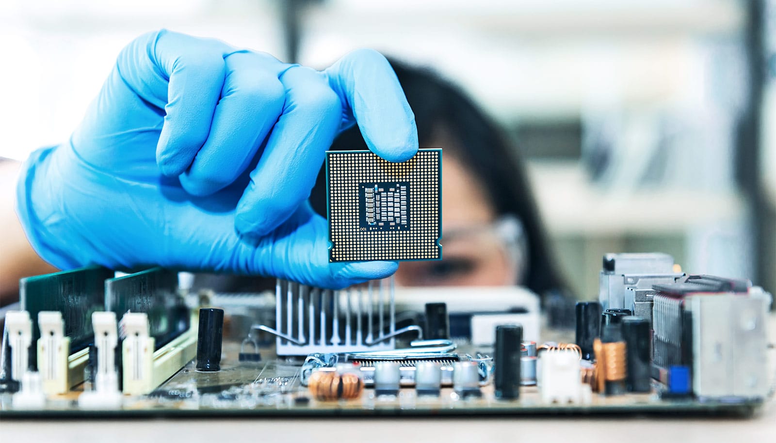
Ultra-compact, yet high-performing electronic chips could overcome the challenges that face conventional integrated circuits and maintain Moore’s Law indefinitely, researchers say.
To create the chips, researchers would take advantage of relatively new and promising two-dimensional (2D) materials and combining them with monolithic 3D (M3D) integration practices.
Moore’s Law says that the number of transistors on a microchip will double roughly every two years. And, thanks to advances in miniaturization and performance, this axiom has held true since 1965, when Intel cofounder Gordon Moore first made that statement based on emerging trends in chip manufacturing at Intel.
However, integrated circuits (IC) are hitting hard physical limits that are rendering Moore’s Law obsolete—elements on a dense integrated circuit can get only so small and so tightly packed together before they begin to interfere with each other and otherwise lose their functionality.
“Apart from fundamental physical limits to the scaling of transistor feature sizes below a few nanometers, there are significant challenges in terms of reducing power dissipation, as well as justifying the incurred cost of IC fabrication,” says Kaustav Banerjee, a professor of electrical and computer engineering at the University of California, Santa Barbara. As a result, the very devices that we rely on for their steadily improving performance and versatility—computers, smartphones, internet-enabled gadgets—would also hit a limit, he says.
While Banerjee first disclosed the idea to combine 2D materials and 3D integration practices in a article back in 2014, more detailed research evaluating this technology from his Nanoelectronics Research Lab now appears in the IEEE Journal of the Electron Devices Society.
“Two-dimensional materials can be stable in their monolayer form with atomic scale thickness—0.5 nanometer or 5 Angstroms for graphene (a conductor) and hexagonal-boron-nitride (an insulator), and ~6.5 Angstroms for 2D transition metal dichalcogenides (semiconductors) such as molybdenum-disulphide (MoS2) or tungsten-disulphide/diselenide (WS2/WSe2),” Banerjee says.
“In addition, due to their layered nature, they offer pristine surfaces relatively free of defects and are excellent conductors of heat in the in-plane direction. All these properties, along with the possibility to directly synthesize these materials on top of prefabricated devices, offer unprecedented advantages over conventional 3D ICs that are already in the market or M3D integration with conventional electronic materials.”
Extending Moore’s Law
According to the Banerjee Group’s study, there’s a limit to how thin conventional semiconductor materials can get before their desirable electronic properties begin to fade.
“Thickness scaling of common semiconductor materials, such as Si, becomes challenging below a few nanometers due to rapid degradation of their mobility caused by the increase in electron scatterings from surface roughness,” Banerjee says. “In fact, below ~1 nm, conventional materials like Si or Ge may not be thermodynamically stable.”
On the other hand, atomically thin and stable 2D materials, such as graphene, hexagonal boron nitride (h-BN), and transitional metal dichalcogenides (MoS2, WS2, WSe2, etc) are highly space-efficient, thickness-wise. Moreover, due to their layered nature and pristine interfaces, the 2D semiconductors exhibit reasonably high mobilities and immunity against surface defects, according to the paper.
In addition, 2D materials tend to be a lot more flexible than their conventional counterparts, which make them ideal for state-of-the-art electronics applications, such as flexible displays. Stacked 2D materials, in contrast to their stacked 3D counterparts, meanwhile, can also minimize the inter-tier signal delays, thermal resistance, and reduce potential overheating.
By selecting certain 2D materials and stacking them, according to the researchers, not only does the monolithic 3D conserve precious space on the chip, but also allows for configuration based on the combined electronic properties of the materials.
“For example, owing to the atomically-thin vertical dimensions of 2D materials, and carefully-designed inter-tier electrostatics with graphene shielding layer that also benefits from enhanced heat dissipation, aggressive scaling of tier thickness down to sub-μm can be achieved,” Banerjee says. “Such scaling allows over 10-folds higher integration density with respect to conventional 3D integration, and over 150% greater integration density with respect to conventional M3D integration, with plenty of room for further improvements.
“Thus, 2D materials can help realize the ultimate density scaling of integrated electronics—both laterally and vertically—which can usher an unprecedented era of innovation and economic growth for the worldwide semiconductor industry,” he adds.
The ‘chip cities’ of the future
As with many innovations with potential to become mainstream technologies, there are challenges to consider to pave the way toward their mass manufacturing. For monolithic 3D devices, the challenges are to be able to fabricate these components at relatively low temperatures (lower than 500 degrees Celsius) to avoid degradations and damages to prefabricated devices located in the lower tiers, electromagnetic interference, and heat dissipation.
Last year, Banerjee’s group demonstrated a CMOS compatible graphene synthesis method that essentially addressed the low-temperature and transfer-free synthesis challenge for graphene. Similar efforts are underway in his laboratory to synthesize other 2D materials directly on wafers at low temperatures.
“Additionally, careful design is needed to electrically shield the generated electromagnetic waves from affecting the operations of devices on adjacent or nearby tiers,” says lead author Junkai Jiang, recent recipient of a doctoral degree in electrical and computer engineering from Banerjee’s laboratory. The researchers note that by using a thin graphene shielding layer between tiers (preferably doped to enhance electromagnetic screening effect), interference can be prevented even as the vertical layers are scaled down.
In terms of heat dissipation, the thinness of the material itself is conducive to allowing the heat from densely packed stacked components to dissipate efficiently. Coauthor Kamyar Parto, a member of Banerjee’s lab, remarked that “the 2D materials have much higher in-plane thermal conductivity compared to thinned-down conventional materials like silicon, which helps fast lateral heat transport, thereby reducing the risks of any hot-spot formation.”
“Ultimately, we envision heterogeneously integrated devices and technologies enabled by 2D materials to realize the world’s tallest and densest ‘chip-cities’ with unprecedented performance, storage capacity, and energy-efficiency,” he adds.
Source: UC Santa Barbara


