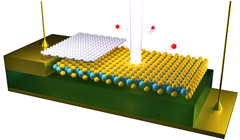
The first visualization of the electronic structure in a microelectronic device may open up opportunities for finely tuned, high-performance devices, report researchers.
Physicists developed a technique to measure the energy and momentum of electrons in operating microelectronic devices made of atomically thin—so-called 2D—materials.
Using this information, the researchers created visual representations of the electrical and optical properties of the materials to guide engineers in maximizing 2D materials’ potential in electronic components.

The study could also pave the way for the types of 2D semiconductors that are likely to play a role in the next generation of electronics, in applications such as photovoltaics, mobile devices, and quantum computers.
Watching electrons in 2D materials
The electronic structure of a material describes how electrons behave within that material, and therefore the nature of the current flowing through it. That behavior varies depending upon the voltage—the amount of “pressure” on its electrons—applied to the material, and so changes to the electronic structure with voltage determine the efficiency of microelectronic circuits.
These changes in electronic structure in operating devices are what underpin all of modern electronics. But until now there has been no way to directly see these changes to help us understand how they affect the behavior of electrons.
Their technique used angle-resolved photoemission spectroscopy, or ARPES, to “excite” electrons in the chosen material.
“It used to be that the only way to learn about what the electrons are doing in an operating semiconductor device was to compare its current-voltage characteristics with complicated models,” says co-corresponding author David Cobden, a professor of physics and faculty member in the Molecular Engineering & Sciences Institute at the University of Washington.
“Now, thanks to recent advances, which allow the ARPES technique to be applied to tiny spots, combined with the advent of two-dimensional materials where the electronic action can be right on the very surface, we can directly measure the electronic spectrum in detail and see how it changes in real time.”
‘This changes the game’
By applying this technique, scientists will have the information they need to develop “fine-tuned” electronic components that work more efficiently and operate at high performance with lower power consumption. It will also help in the development of 2D semiconductors that scientists see as potential components for the next generation of electronics, with applications in flexible electronics, photovoltaics, and spintronics. Unlike today’s 3D semiconductors, 2D semiconductors consist of just a few layers of atoms.
“How the electronic structure changes with voltage is what determines how a transistor in your computer or television works,” says co-corresponding author Neil Wilson, an associate professor of physics at the University of Warwick. “For the first time we are directly visualizing those changes. Not being able to see how [structure] changes with voltages was a big missing link. This work is at the fundamental level and is a big step in understanding materials and the science behind them.”
By focusing a beam of ultraviolet or x-ray light on atoms in a localized area, the excited electrons get knocked out of their atoms. Scientists can then measure the energy and direction of travel of the electrons, which—thanks to laws for the conservation of energy and momentum—allows them to work out the energy and momentum they had within the material. That determines the electronic structure of the material, which researchers can then compare against theoretical predictions based on state-of-the-art electronic structure calculations coauthor Nicholas Hine’s group at the University of Warwick performed.
“This powerful spectroscopy technique will open new opportunities to study fundamental phenomena, such as visualization of electrically tunable topological phase transition and doping effects on correlated electronic phases, which are otherwise challenging,” says co-corresponding author Xaiodong Xu, a professor of both physics and materials science and engineering, as well as faculty member in the Clean Energy Institute.
The team first tested the technique using graphene before applying it to 2D transition metal dichalcogenide, or TMD, semiconductors.
“The new insight into the materials has helped us to understand the band gaps of these semiconductors, which is the most important parameter that affects their behavior, from what wavelength of light they emit, to how they switch current in a transistor,” says Wilson.
“This changes the game,” says Cobden.
The research appears in the journal Nature.
Additional researchers are from the University of Washington, the University of Warwick, Elettra–Sincrotrone Trieste, and the University of Cambridge. The US Department of Energy, the UK Engineering and Physical Sciences Research Council, the National Science Foundation, the University of Warwick, the Winton Programme for the Physics of Sustainability, the Cambridge Trust European Scholarship, and the University of Cambridge funded the research. The researchers took measurements at the spectromicroscopy beamline at the Elettra–Sincrotrone Trieste.
Source: University of Washington


